Low-latency Ethernet market-data decoder
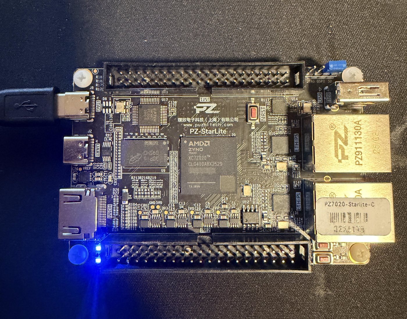
SystemVerilog on a Xilinx Zynq-7020, July 2026 to now
In shortCustom digital hardware on an FPGA (a reprogrammable chip) that reads stock-exchange messages straight off an Ethernet cable and decodes each one in about 73 nanoseconds in simulation.
A Nasdaq TotalView-ITCH 5.0 parser that takes raw Ethernet off the wire and hands out decoded order-book messages, entirely in FPGA fabric.
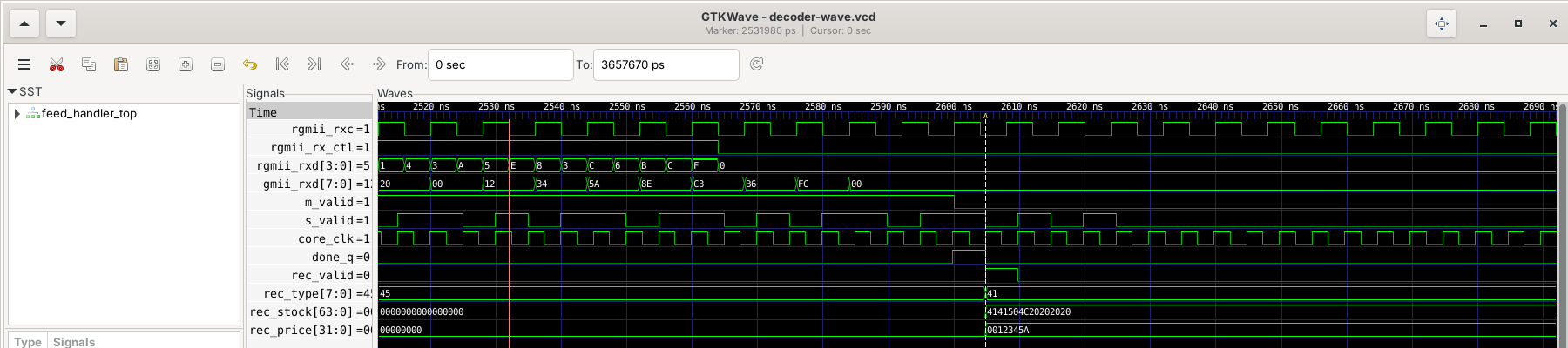
- I wrote the Ethernet MAC, IPv4/UDP and MoldUDP64 parsers to work cut-through: fields are decoded while the frame is still arriving, and a bad checksum at the end rolls the work back.
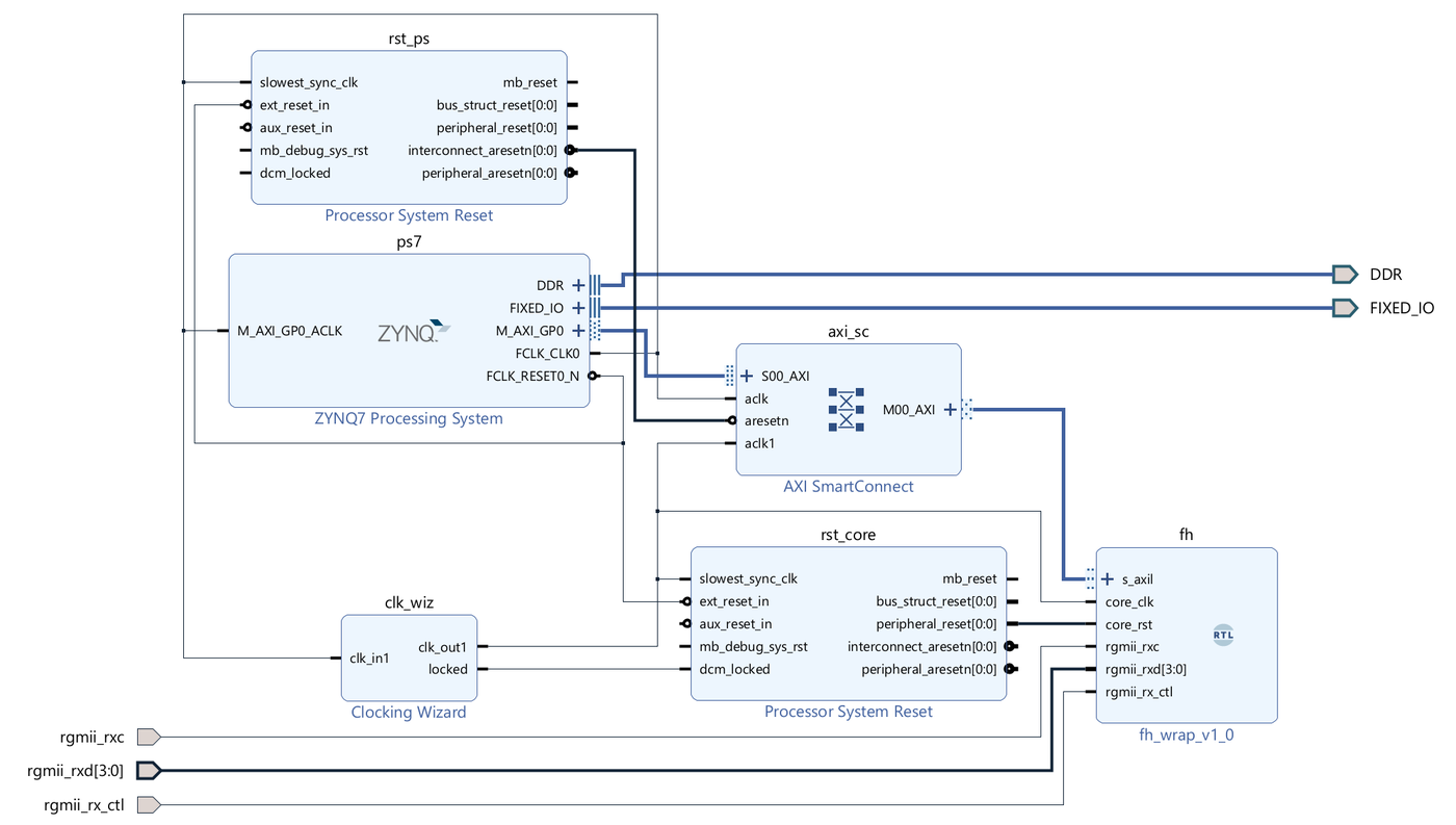
- I designed a Gray-coded async FIFO to carry data from the 125 MHz PHY clock to the 200 MHz core clock, and sized it from the clock ratio and frame length.
- I built a 10-test cocotb regression that compares the RTL against a Python golden model, with fault injection: 7,430 records, zero mismatches.
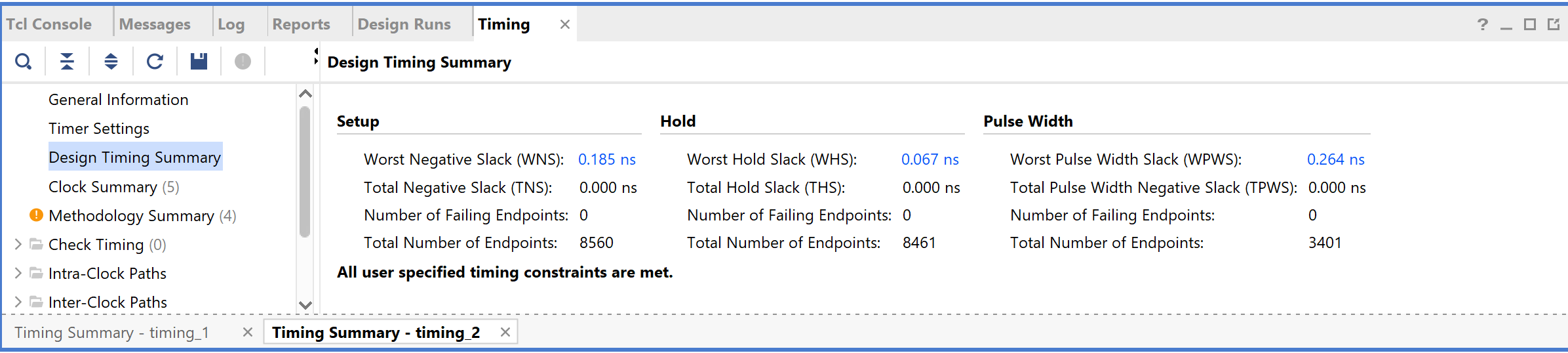
- I scripted the Vivado build in Tcl, captured RGMII with IDELAYE2/IDDR and BUFIO/BUFR clocking, and closed timing at 200 MHz (WNS +0.185 ns).
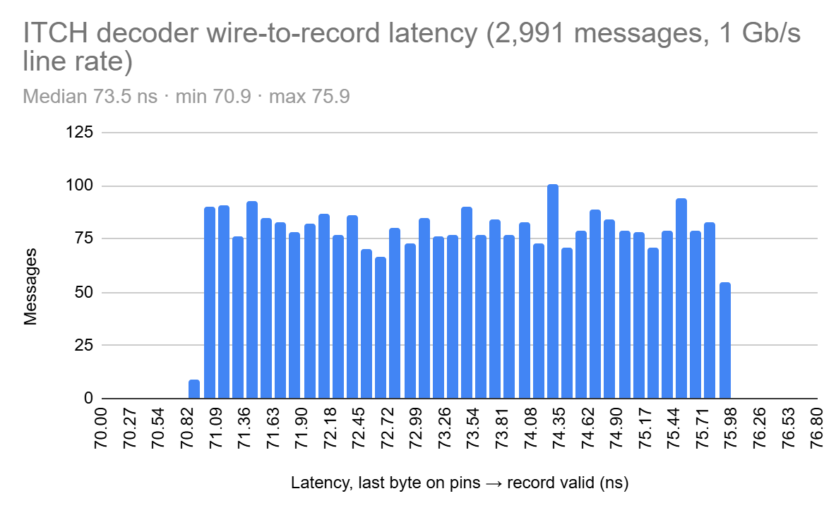
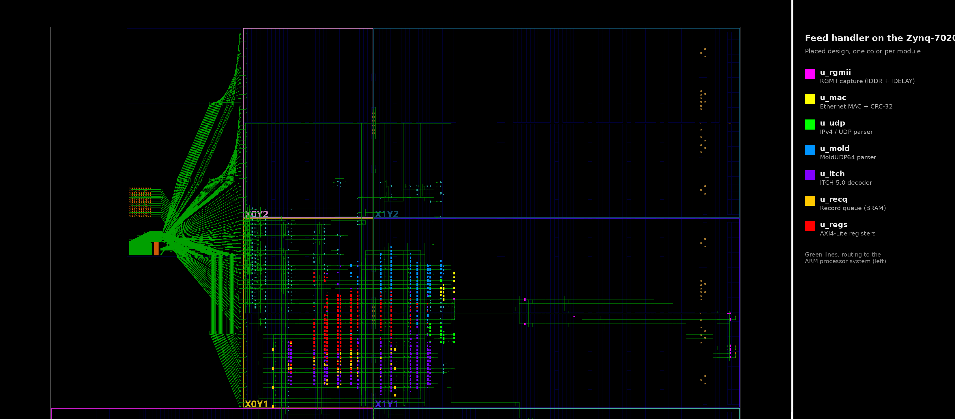
- Median latency, pin to record
- 73.5 ns sim
- Throughput
- 3.39M msg/s line rate
- Timing at 200 MHz
- WNS +0.185 ns
- Device use
- 3.4% 1,824 LUT, 2,459 FF
RV32IM five-stage pipelined RISC-V core
SystemVerilog on a Xilinx Zynq-7020, March to July 2026
In shortA processor I designed from scratch: it runs standard RISC-V programs, passes all 48 official tests, and matched a reference simulator over 12.5 million instructions.
An in-order CPU that runs real RISC-V programs on the FPGA, with the Zynq's ARM core loading programs and acting as the console.
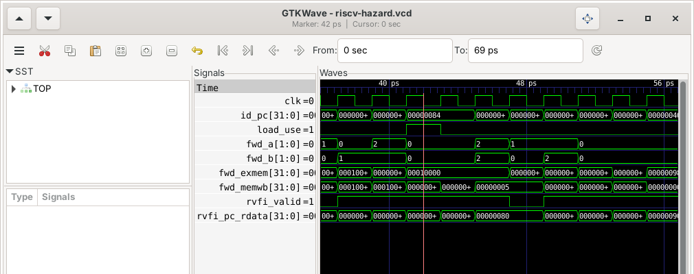
- I designed the five-stage pipeline with full operand forwarding, a load-use interlock and precise exceptions (Zicsr).
- I built the multiplier on DSP48 slices, pipelined so it doesn't limit the clock.
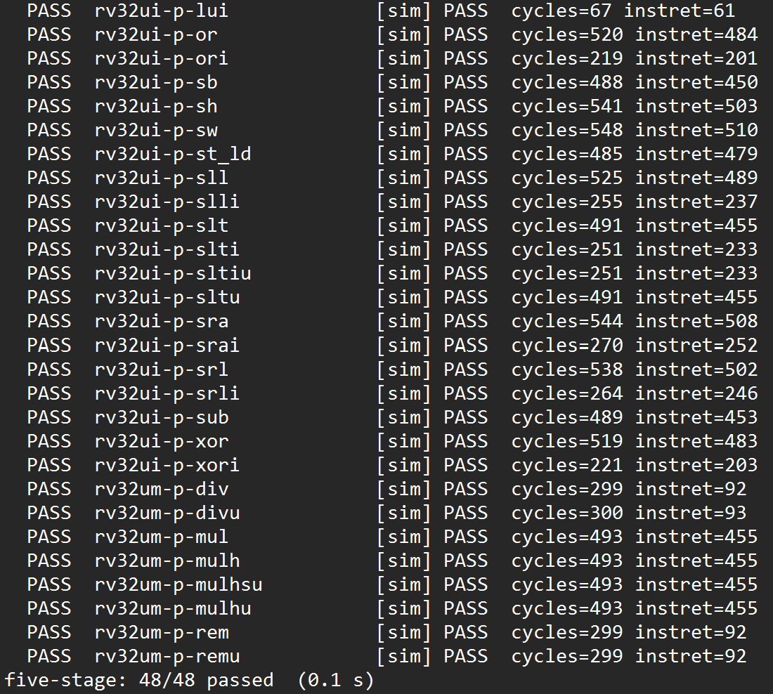
- I set up the verification: the official riscv-tests and RISCOF suites, plus an instruction-by-instruction lockstep check against the Spike reference simulator.
- I benchmarked it with CoreMark in simulation, with a CPI breakdown from hardware performance counters.
- Performance
- 2.857 CoreMark/MHz
- CPI on CoreMark
- 1.117
- Compliance
- 48 / 48 riscv-tests
47 / 47 RISCOF - Lockstep with Spike
- 12.5M instructions, 0 divergences
NanoGuard: FPGA pre-trade risk checks you can change in minutes
Rutgers TechStart 2026, finalist (top 5 of the competition), team of six
In shortA startup prototype, and top-5 finalist at Rutgers TechStart 2026, that lets compliance staff change hardware trading-risk checks in plain English instead of waiting weeks for engineers.
Brokers with direct market access must check every order before it reaches the exchange (SEC Rule 15c3-5). FPGA checks are fast, but changing a rule takes weeks of engineering. NanoGuard was my idea for closing that gap, and I built the working prototype we demoed live to the judges.
- I wrote the Verilog risk-check module: restricted list, max order size, price collar and capital limit, in a 2-stage pipeline with configurable registers.
- I built the Python pipeline: the LLM rule builder with a constrained tool schema, a validator against the template catalog, a compiler to register values, and the approval step.
- I verified the RTL against a Python reference model on 100,000 random orders, with zero mismatches, and built the Streamlit demo we ran on stage.
- AI proposesA compliance officer types a rule in plain English. An LLM maps it to a pre-verified hardware template.
- Tests verifyThe rule is compiled to register values and checked in simulation with Icarus Verilog.
- A human approvesNothing reaches the hardware without sign-off. Out-of-scope requests become engineering tickets.
- Hardware enforcesThe FPGA checks every order in about 2 clock cycles. The AI is never in the trading path.

AeroBin: a clip-on fill-level sensor for any waste container
Custom ESP32-C3 board in KiCad, Verizon Smart Campus Competition 2026–27
In shortA circuit board I designed for a clip-on sensor that reports how full a waste container is, for the Verizon Smart Campus Competition.
AeroBin clips onto a bin that's already in place and reports how full it is, so pickups happen when a container needs one instead of on a fixed schedule. It won first place in last year's Verizon Smart Campus Competition, which took the team to Verizon headquarters. This year we're building it to track any waste container and to earn real revenue for Verizon. We're developing it with Verizon's engineering mentors, and Qualcomm has offered its technology to help.
- I defined the hardware architecture and chose the sensor, power path and microcontroller.
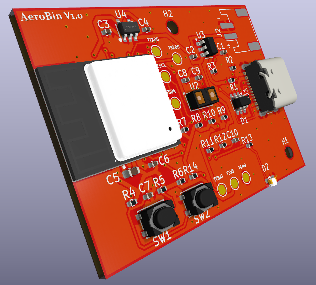
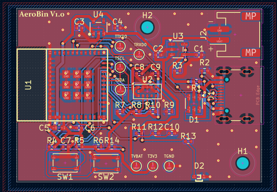
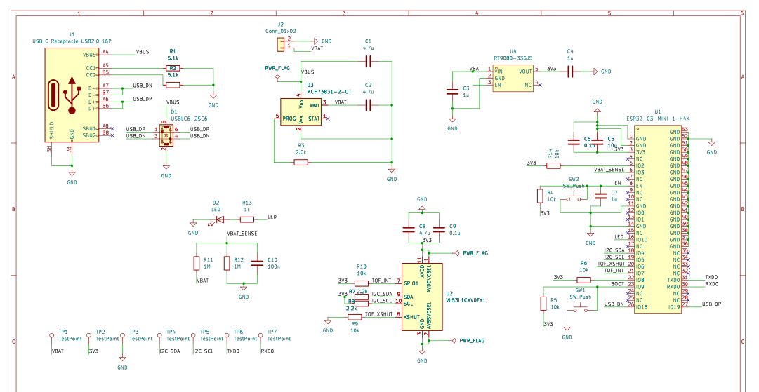
- I designed the V1 board in KiCad: a 45 × 32 mm two-layer PCB around an ESP32-C3-MINI-1 module, with a VL53L1CX time-of-flight sensor on I²C that measures the distance down to the waste.
- I built the power path: USB-C input with USBLC6 ESD protection, an MCP73831 Li-Po charger, a JST-PH battery connector, an RT9080 3.3 V regulator, and a divider so the firmware can read the battery voltage.
- I designed it for bring-up: seven labeled test points (3V3, VBAT, GND, UART TX/RX, I²C SCL/SDA), BOOT and EN buttons, a status LED, and native USB for flashing.
- I'm designing the 3D-printed enclosure the board mounts in.
V1 connects over Wi-Fi so we can demo a working unit now; the product is planned to run on Verizon LTE-M.
- Board
- 45 × 32 mm 2 layers, 1.6 mm
- Parts
- 41 placed
- Routing
- 558 tracks, 101 vias
- Status
- Routed awaiting fab
- A line per containerEach AeroBin is planned to run on its own Verizon LTE-M line, so every container we track is another paid connection.
- Any containerIt clips onto bins, dumpsters and recycling containers that are already deployed, so the number of lines grows with every site.
- Copper and device recyclingWe're targeting the containers that collect copper and old devices for recycling. The copper telecom companies are pulling from retired networks alone is worth over $7 billion, by one industry estimate.
Other boards and builds
Printed circuit boards and robotics from team projects
In shortOther circuit boards and builds from my student engineering teams: the solar car and a lunar mining robot.
| Ref | Build | What I did | Status |
|---|---|---|---|
| PCB1 | AeroBin sensor board Verizon Smart Campus Competition | Custom ESP32-C3 board in KiCad and a 3D-printed enclosure for a clip-on fill sensor. Detail sheet PCB1. | Awaiting fab |
| PCB2 | LV3 Core carrier board Rutgers Solar Car | Designed the STM32G4 mixed-signal board for battery telemetry and protection: reverse-polarity protection, voltage sensing, buck regulation. Brought it up on the car. | Built |
| NET1 | Low-voltage CAN network Rutgers Solar Car | Engineered a daisy-chained FDCAN topology linking 8 boards for real-time data between the battery managers and peripherals. | Built |
| PCB3 | Lunabotics robot controller Space Technology Association of Rutgers | Designed the board linking a Jetson Nano to sensors and motor controllers; wrote C and Python motor control and SLAM navigation on ROS 2. | Built |
Crusoe: data center facility operations
Facility Operations intern, May to August 2026, San Francisco, CA
In shortMy summer internship at an AI data center company, where I mapped a site's power and cooling equipment and worked on giving each piece one name every system agrees on.
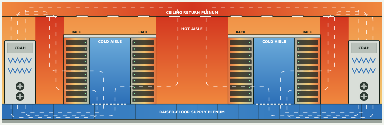
Crusoe builds and runs AI data centers. I worked across the reliability, controls and commissioning teams. Most of my summer went to one problem: the same piece of equipment had a different name in the maintenance system, in SCADA and in the cloud dashboards, so nothing could be matched automatically.
- Asset map
- 716 assets
- Naming standard
- 5 levels from 7
- Tag parser
- 23 unit tests
- Equipment lists
- 12 missing types found
- I built the asset map for a deployed modular site: 716 electrical, mechanical, security and life-safety assets, each linked to the asset that feeds it, so the power path from substation to rack PDU can be walked without opening a drawing.
- I proposed a five-level naming standard for modular sites, adapted from a seven-level standard written for large buildings, and measured row by row how far the live SCADA tags sat from it.
- I wrote a Python tag parser that flattens nested SCADA/MQTT telemetry tag exports (JSON) into a CSV any engineer can open in Excel, cutting on-site processing from hours to minutes, with 23 unit tests and a plain-language guide for non-programmers.
- I built a commissioning scope-of-work RFP for two new buildings of a GPU data center campus, and a validation matrix that checks equipment lists against the drawing schedules in both directions. It found 12 equipment types missing from the original lists.
- I evaluated ML and reinforcement-learning approaches for the predictive control layer of a data center digital twin, and modeled the cost of physics-only vs hybrid training.
The drawings are generic illustrations: no site photos, layouts or internal data.
Experience
An internship, two engineering teams, and earlier work
In shortWhere I've worked: a data center internship, two student engineering teams, and earlier jobs in ECG signal analysis and car electronics.
May to August 2026
San Francisco, CA
Data Center Facility Operations Intern
- Built a Python tag parser that flattens nested SCADA/MQTT telemetry tag exports (JSON) into clean CSV datasets, cutting on-site processing from hours to minutes; 23 unit tests.
- Proposed a five-level naming standard for modular sites so maintenance records, SCADA tags and cloud dashboards share one name per asset, and measured the live SCADA tags against it.
- Built the asset map for 716 electrical, mechanical, security and life-safety assets, each linked to the asset that feeds it, from substation to rack PDU.
- Wrote a commissioning scope-of-work RFP for two new GPU data center buildings and a validation matrix that found 12 equipment types missing from the original equipment lists.
- Evaluated ML and reinforcement-learning approaches for the predictive control layer of a closed-loop data center digital twin, and modeled cost tradeoffs between physics-only and hybrid physics+ML training.
September 2024 to now
Piscataway, NJ
Low Voltage Systems Engineer
- Engineered a daisy-chain FDCAN topology linking 8 distributed system boards, enabling reliable real-time data exchange between high/low-voltage managers and peripheral modules.
- Designed the “LV3 Core” mixed-signal carrier PCB (STM32G4 MCU) for low-voltage battery telemetry and protection.
- Implemented reverse-polarity protection, voltage-sensing telemetry and buck-converter regulation, then validated signal integrity and I/O pin mapping during hardware bring-up.
September 2024 to now
Piscataway, NJ
Software/Controls Engineer
- Designed a custom PCB interfacing an NVIDIA Jetson Nano onboard computer with peripheral sensors and motor controllers, engineering signal-routing and power-distribution circuitry for reliable multi-sensor operation.
- Developed C/Python control logic and motor-driver controls for a NASA Lunabotics lunar mining robot on Linux.
- Implemented SLAM-based 3D perception and autonomous navigation using a Unitree 4D Lidar L2 and ROS 2.
Other work experience
Earlier jobs outside digital design.
July 2025 to February 2026
Full-time
New Providence, NJ
ECG Data Analyst and Technician
How it connects: this was signal-processing work. Every scan is a sampled waveform where real events have to be separated from noise and motion artifacts, and the ML models had to be checked against known answers, the same discipline as verifying hardware against a reference model.
- Analyzed 200+ ECG scans a month, applying digital signal processing concepts to identify cardiac arrhythmias and signal artifacts.
- Validated BDx software by generating test cases for CNN-RNN machine-learning models that automate the classification of abnormal heart rhythms (PACs and PVCs).
- Kept diagnostic reports clinically accurate by telling true cardiac events from motion artifacts through waveform pattern recognition.
June 2022 to March 2024
Paterson, NJ
Automotive Hardware Apprentice
- Installed aftermarket electronics in 10+ vehicles, integrating head units and wiring modules for Apple CarPlay and Android Auto.
- Fabricated custom mounting brackets and wiring harnesses with 3D printing and AutoCAD for secure component fit.
- Serviced HVAC and electrical systems: crimping, soldering and schematic tracing for sensor repairs.
Toolbox
In shortThe languages, design tools and lab skills I use.
RTL and FPGA
Verilog and SystemVerilog, synthesis, timing closure, clock-domain crossing, functional verification. Vivado, ILA, cocotb, Verilator, Yosys.
Interfaces
Ethernet MAC (RGMII/GMII, FCS/CRC-32), UDP/IPv4, MoldUDP64, AXI4-Lite, FDCAN.
Programming
C, Python, Tcl, RISC-V assembly, MATLAB, Java, SQL, Linux, Git, ROS 2.
Boards and lab
KiCad, LTSpice, mixed-signal design, SolidWorks and Onshape, oscilloscopes, soldering, 3D printing.
Get in touch
Open to Summer and Fall 2027 internships in FPGA, RTL, ASIC and verification.
ubrahin17@gmail.com

- Rutgers University–New Brunswick · B.S. Electrical Engineering, minor in Computer Science · Class of 2028
- Honors College · Engineering Honors Academy · Dean's List
- New Brunswick, NJ